The inclusion of nonlinear optical functions in integrated optics has recently generated considerable interest. The potential for integrated photonic systems has been demonstrated in demonstrations. Furthermore, the development of fully integrated, nonlinear optical devices aimed at various applications, such as all-on-chip spectroscopy, on-chip quantum computations, and communications, efficient multiplexing for data communications, on-chip metrology, bio-sensing, or LIDARs, has been motivated by large-scale manufacturing capability and affordability.
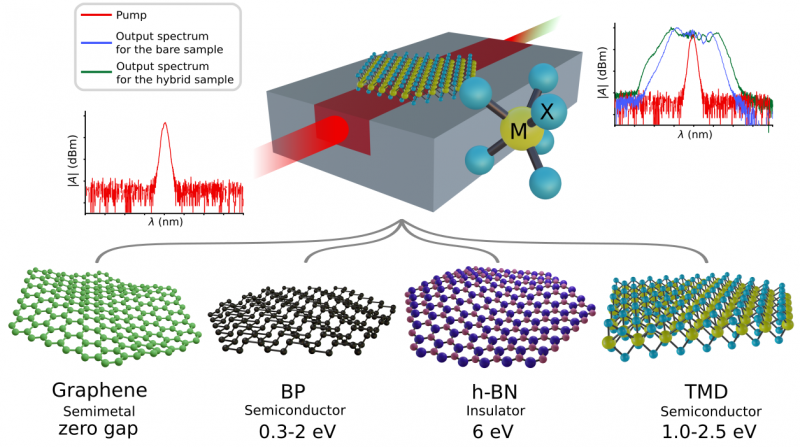
Figure | Principle of the hybrid integration of 2D materials on photonic waveguides. Image Credit: Light: Advanced Manufacturing
A team of scientists led by Professors Vincent Pelgrin and Zhipei Sun studied the spectrum of hybrid photonic integration structures in a new study published in Light: Advanced Manufacturing.
Integrating these many active functionalities in silicon photonics has also received a lot of attention. The platform’s potential interoperability with CMOS technologies, as well as its generally low cost, makes it particularly appealing to industry, with components immediately suitable for dense optical circuit construction.
Due to its comprehensive integration capabilities, the Si-compatible platform is an intriguing testbed for transposition. When it comes to using nonlinear optical processes, silicon photonics offers several challenges. These are essentially the modest nonlinear reactions of the most commonly used materials to clean room techniques or the presence of free carriers.
Si is extremely nonlinear in the C-band area yet suffers from Two-Photon Absorption (TPA) due to its small bandgap. Unfortunately, most traditional materials suitable for silicon integration are weak in terms of optical nonlinearities. The stochiometric SiN nonlinear refractive index (n2) is about two orders of magnitude lower than Si. The stochiometric SiN nonlinear refractive index (n2) is about two orders of magnitude lower than Si.
Various silicon-based materials have been used to produce integrated optical capabilities in impressive demonstrations. Supercontinuum generators, frequency combs, and photon pair sources via spontaneous four-wave mixing are among them. In various industries, groups have pushed for more efficient technologies that provide excellent performance while consuming minimal energy.
Although annealed SiN waveguides with loss levels of a few dB/m have been developed, the required pump power remained high. To obtain adequate nonlinear processes, long waveguides were required, making optical functions difficult for fully integrated systems.
Materials such as Si-rich waveguides or employing p-i-n junctions to tailor carrier density have also shown interesting results. However, there are some downsides. TPA can still be found in Si-rich waveguides. At the same time, employing several p-i-n junctions adds another layer of complexity to devices and circuits. As a result, the demand for remedies to this constraint remains acute.
Another strategy is to incorporate highly nonlinear materials into the on-chip platform to benefit from their very effective features. Through the integration method, this approach improves their nonlinear performance. Several materials have been evaluated throughout the last decade.
Chalcogenides are a common substitute for Si-based products. Two-dimensional (2D) layered materials have been found to be particularly promising in the search for disruptive nonlinear optical materials. Third-order susceptibility in these materials is up to two orders of magnitude more than in Si.
The most well-known material in this group is graphene. Other 2D materials include Transition Metal Dichalcogenide (TMDs). MX2 crystals are named after metal atoms (M) and chalcogens (X). BP is also gaining popularity.
The concept behind hybrid integration is to include high-performance 2D materials into current integration platforms, hence boosting the total effective nonlinear performance of the waveguides.
As 2D materials are still poorly understood, the hybrid integration strategy presents several obstacles. The impact of their incorporation into integrated structures must be carefully considered. The review summarizes current advancements in the field as well as the team's concepts.
They provided a brief theoretical overview of the hybrid integration of 2D materials for the various integrated optics systems. The goal is to describe important phases, from modeling and design through characterization. This will ideally serve as a roadmap for future research in related domains, removing one of the barriers to integrated nonlinear photonics.
The Centre for Nanoscience and Nanotechnology (C2N) at Paris Saclay University in France, Aalto University in Finland, the Academy of Finland, the Academy of Finland Flagship Program, the EU, and the ERC all provided funding for the study.
Journal Reference
Pelgrin, V., et al. (2023) Hybrid integration of 2D materials for on-chip nonlinear photonics. Light: Advanced Manufacturing. doi:10.37188/lam.2023.014
Source: https://www.cas.cn/